

Process: texturing (INTEX)→diffusion (DIFF)→post-cleaning (cutting/removing PSG)→anti-reflection coating (PECVD)→screening, sintering (PRINTER)→testing, sorting (TESTER+SORTER)→packaging (PACKING)
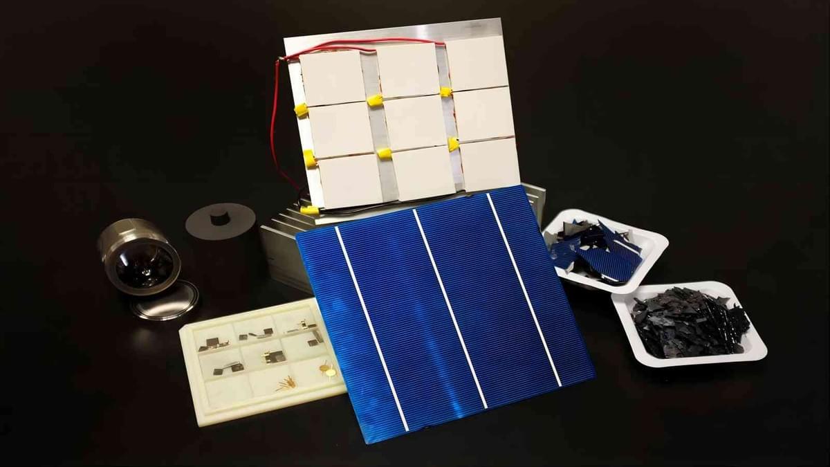
1.PV panel Cell texturing
The formation of a rough surface on the silicon wafer's surface is done to lessen the cell's reflectivity. Secondary reflection is amplified and the optical path and incident mode are altered due to the surface's textural irregularities. Pyramid-shaped suede can be made by treating a single crystal with alkali, while wormhole-shaped random suede can be made by treating a polycrystal with acid. The primary distinction between the two processing approaches is in the characteristics of single polycrystalline
Technical procedure: cashmere in tank, water washing, water washing, acid washing, water washing, drying.
When exposed to HF and HNO3, silicon's surface becomes passivated and is hence non-reactive. Silicon undergoes a continual reaction with a mixed solution of two acids when it is present in the system.
2. Diffusion of PV panel cells
The P-N junction and battery's beating heart are both products of diffusion. At present, phosphorus diffusion is achieved via POCl3. Since POCl3 is a liquid phosphorus source, diffusion of this material results in improved production efficiency, stability, PN junction smoothness, and diffusion layer quality.
Above 600 °C, POCl3 decomposes into PCl5 and P2O5, two different phosphorus compounds. Silicon wafers can have their surfaces damaged by PCl5. PCl5 breaks down into P2O5 and chlorine gas in the presence of oxygen (O2). As a result, nitrogen is released into the atmosphere while oxygen is added in a measured stream.
P2O5 interacts with silicon at the diffusion temperature, creating silicon dioxide (SiO2) and phosphorus atoms. The P2O5 that forms as a byproduct is deposited on the silicon wafer's surface, where it continues to react with silicon to produce more SiO2 and phosphorus atoms. Phosphorus-silicate glass (PSG) is what forms on the silicon wafer during this procedure.
When phosphorus atoms diffuse into silicon, an N-type semiconductor is formed.
3. Etching of PV panel cells
Phosphorus atoms diffuse along the sides and rear of the silicon wafer thanks to the back-to-back single-sided diffusion technique used during the procedure.
Electrons created by light and collected on the front side of the P-N junction travel to the back side when sunlight is present, creating a short circuit in the region where phosphorus is diffused along the edge.
Parallel resistance is decreased when the channel is shorted.
To prevent a short circuit of the P-N junction and lower the parallel resistance, the etching procedure seeks to eliminate the phosphorus region on the edge of the silicon wafer.
Film is loaded, then washed, then etched with H2SO4, HNO3, and HF, and finally rinsed in alkali and HF baths before being removed.
SiO2 is produced via an HNO3-oxidation reaction, while SiO2 is removed via HF. The process of etching in an alkaline tank makes the previously untextured surface consistent and smooth. KOH is the primary solution in the alkali tank. H2SO4 is utilised to make the assembly line run more smoothly by lubricating the silicon wafers, but it does not contribute to the reaction itself.
Dry etching is plasma etching of thin films. The plasma state of a gas increases its chemical activity.
The silicon wafer can undergo etching quickly by using the right gas. In addition to directing and speeding up the plasma, the electric field also provides it with energy. By transferring physical energy, the atoms of the silicon material are displaced when the wafer's surface is attacked, resulting in etching.
4. PECVD
A thin film is deposited on the surface of silicon using plasma chemical vapour deposition (PCVD). About 35% of the light that strikes silicon is reflected. Applying an anti-reflection coating allows the solar cell to absorb more light. This film improves conversion efficiency by increasing the photo-generated current. Surface recombination at the emitter junction is also decreased because of the hydrogen-containing film's passivating effect on the cell. This enhances the effectiveness of photoelectric conversion by decreasing the dark current and raising the open circuit voltage.
Reactions between hydrogen in the film and silicon flaws or impurities are possible. Through this process, energy is transferred from the prohibited band to the valence band or conduction band.
Using a graphite boat as a conductor, a layer of SixNy film is deposited to the surface of the silicon wafer in a vacuum at a temperature of 480 degrees Celsius.
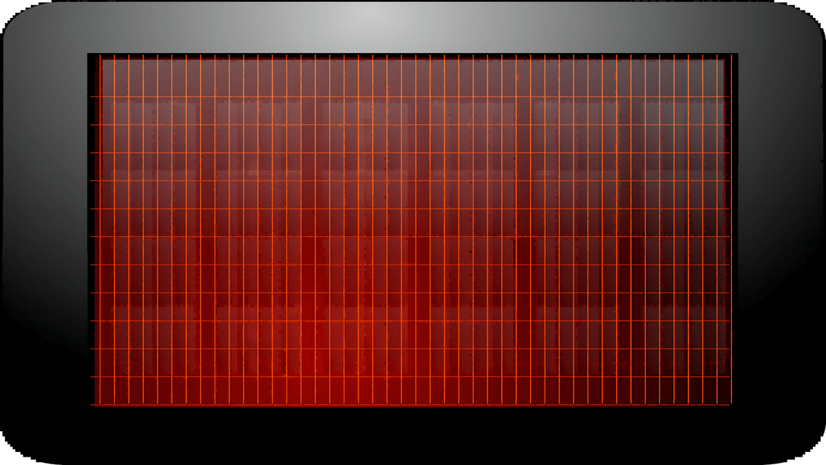
5. Screen printing of PV panel cells
Essentially, it entails amassing electrical current and making solar cell electrodes. The back of the cell is prepared by first applying a silver electrode, and then printing and curing an aluminium back field. Next, a silver front electrode is printed while paying close attention to the sub-grid's wet weight and width.
Too much slurry is wasted and not enough is dried before entering the high-temperature zone if the wet weight of the second step is too high. This can lead to the organic materials still being present in the slurry after the transformation into aluminium metal is complete.
After sintering, the solar cell can bend if it is too heavy. Sintering will not be successful if there is not enough wet weight to use all of the aluminium paste. This creates a silicon alloy region that can't be used for back metal contact. This is due to low solderability and weak lateral conductivity. In addition, it might lead to unsightly lumps and sags.
Reduced efficiency results from a decrease in the light-receiving area of the cell if the width of the third grid line is too large.
Printing method: physical printing, drying
6. Sintering of PV panel cells
Sintering refers to the high temperature heating of the printed electrode on the surface of the cell. The open circuit voltage and fill factor of the cell are both increased as a result of the enhanced electrical contact between the electrode and the silicon chip. It also guarantees a high conversion efficiency by keeping the electrode's resistance low.
Hydrogen diffusion into the PECVD process is aided by sintering. The cell is effectively passivated, which is a bonus.
High temperature fast sintering is employed, with infrared heating providing the necessary heat.
Sintering involves a wide range of physical and chemical interactions, as well as diffusion and flow.
The Ag and Al at the back diffuse into the silicon, whereas the Ag at the front diffuses into the silicon via SiNH but is unable to reach the P-N surface. In order to forge an alloy, a specific temperature must be reached. Ag, Since Al and Si alloys are not equally stable, different temperatures must be used to produce alloying for each element.
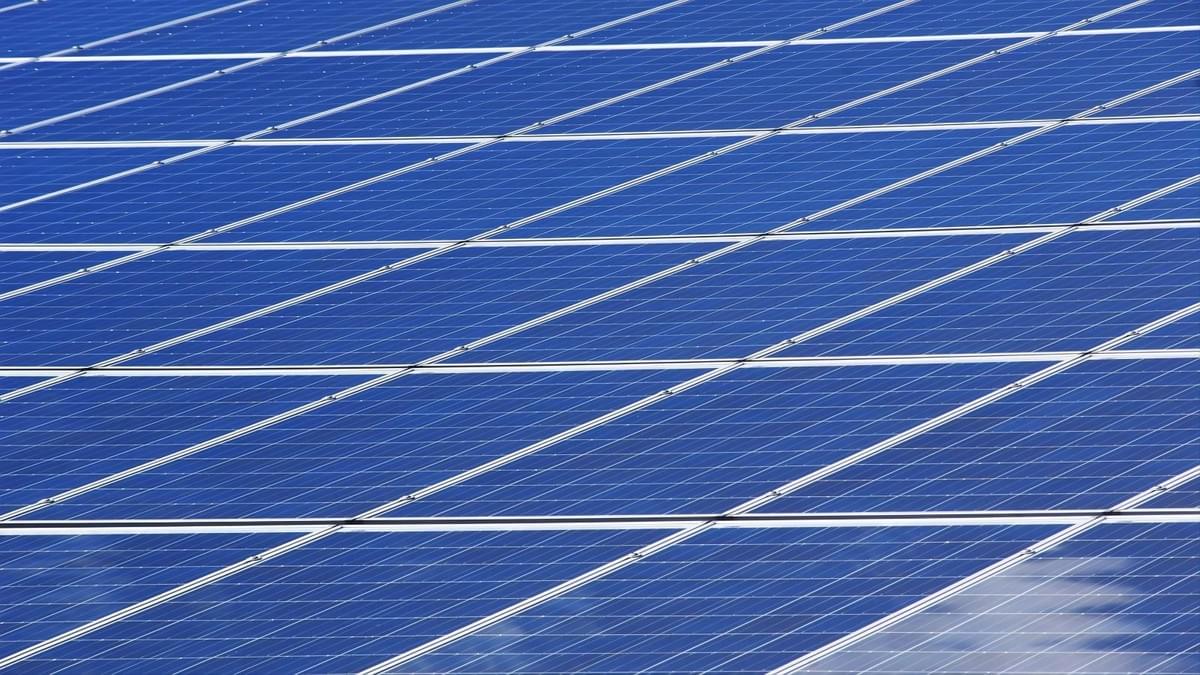
Maysun Solar has been manufacturing solar modules since 2008, and our selection includes several options that make use of PERC technology and are housed in glass modules.
Contact Maysun Solar so that we may work together to build a sustainable future, as we offer the best solar panel technology available.

